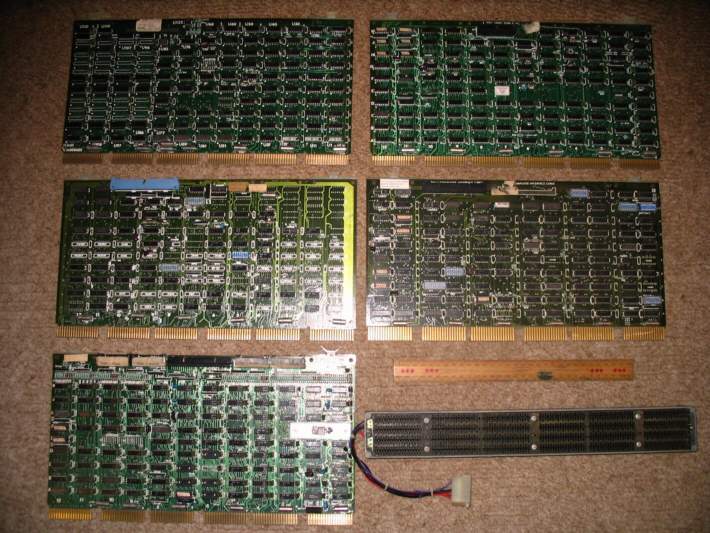
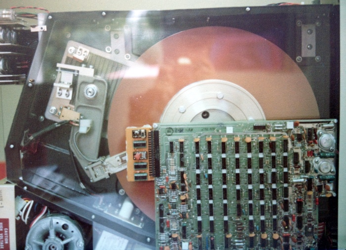
A 5-Board Phoenix 211 Disk Controller
This is one of several pages relating to the history of the automatic totalizator, its invention in 1913, the inventor George Julius and the Australian company he founded in 1917 which became a monopoly, later part of an oligopoly, in this field. This page provides a glimpse at maintaining a PDP11 based tote system. This is a history only non commercial page. If you wish to start from the beginning then go to the index .
Copyright © 2007 Email - totehis@hotmail.com
| PDP11 Based Tote Maintenance |
In the budding years of the 21st century the computer industry is developing so rapidly, that the way it was is being lost. I find it curious that there are now technologists that believe it is not possible to build a computer without a microprocessor.
The Brisbane Project system along with other tote systems of the time existed in an era, 1970s and 80s, when microprocessors lacked the processing speed to run the real-time multi user systems required for the tote transaction processors. Microprocessors existed and were extensively used in controllers and TIMs (Ticket Issuing Machines). The J22 TIMs used with the Brisbane Project utilised the M6800 microprocessor. The PDP11 based tote transaction processors however, instead of having most of the processor's functionality on a single large-scale integrated circuit was implemented using small to medium scale integration providing the required sequential and combinational logic circuits. This implementation required multiple circuit boards just to implement the processor never mind the input/output devices. These systems utilized the TTL (Transistor Transistor Logic) logic family, which was considerably faster than the MOS (Metal Oxide Semiconductor) and CMOS (Complementary Metal Oxide Semiconductor) logic families of the time, which are more suitable for large-scale integration.
The PDP11/34s we used were implemented utilising microcode. The processor was divided into data paths and control section. The heart of the data paths section was the ALU (Arithmetic Logic Unit) with its A and B legs for storing operands for the arithmetic and logic operations as well as providing shift and rotate operations. The control section had a control store ROM (Read Only Memory). The output of the control store, which was 47 bits wide provided the clocking and sequencing signals required to move and manipulate data in the data paths section. By reading contents of the control store ROMs in particular sequences the macro level instructions like the ones in the machine code program below, were executed. In later machines programming languages were developed for writing microcode. This was not for use by programmers however this was the realm of the computer architects and hardware engineers. There is an example of microcode listing in the table below titled Microcode Steps under the heading Some extracts from The Brisbane Fault Logs and sub heading PDP11/34A Processor Fault 26/1/84. It is ironic, as previously stated, that in the latter period of my working life, there were competent engineers who did not believe it was possible to build a digital computer without the use of a microprocessor. The microcode method just described is just one of several methods of designing a digital computer that pre-dated microprocessors.
In this era there was considerable specialisation. Programmers were assembly programmers, higher-level language programmers, system programmers or system managers. Even the higher-level language category became divided with modular, structured, object oriented, rapid prototyping, procedural, event driven... methods. There was some evidence of multi skilling, however I have heard programmers claiming to be out of their realm of expertise on multiple occasions. With specialisation within programmers there obviously was a huge software/hardware divide. We had a broad spectrum programmer once, called Simon. Unusual for a programmer of the time he had a good understanding of the hardware, which made him particularly effective. But even here we came across a conceptual stumbling block. I had written a machine code program like the one below to send a string of characters to a line printer interface to provide a stable set of signals suitable for analysis with a CRO (Cathode Ray Oscilloscope) to determine the cause of an intermittent problem. I was surprised to find that Simon who was being inconvenienced by the problem could not believe that this program did not utilise an operating system. This type of program was called a "Stand-alone Program" a term I have not heard in a long time. It manipulated the hardware I/O (Input Output) registers directly like the drivers of an operating system. I discussed this for a while with Simon however in the end I think he still believed the program was using operating system services to perform the I/O operation. This actually seems odd now as this system was the first tote that Automatic Totalisators built utilising an operating system of any sort in this case RSX11M. In all the predecessors, the tote software was stand-alone and did all the memory allocation/deallocation, interrupt handling, exception handling, queue management etc.
The following PDP11 machine code program was written to establish stable signals (recurrent in a short timebase) suitable for CRO analysis of an intermittent data corruption problem on a DMX, which was a PDP11 based front end processor developed by ATL for use with these tote systems. This program is not an assembler program. It uses assembler mnemonics to make it easier to quickly ascertain what it does. The addresses on the left and the instructions to the right of the mnemonics were manually created and written on a piece of paper using a programming summary card where necessary to provide a forgotten operation code or addressing mode or in particular the base for a conditional branch instruction. The program would need some modification to make it suitable for submission to an assembler. Writing machine code programs was a common practice as you would often be fixing hardware in an environment where no development system with an assembler would be available. Additionally hardware engineers often would be able to write machine code but not use an assembler. Once written, the instructions were manually loaded into the memory locations listed on the left, 16 bits at a time in octal (a numbering system with a base of 8 used in preference to decimal due to its ease of conversion to and from binary (a numbering system with a base of 2) which the processor uses), using the console emulator. In earlier PDP11 processors this was done in binary entering addresses and data using banks of switches. The PDP11 has a 16-bit word length however memory is byte addressable hence the addresses in the left hand column increment by two for every word of memory used. Branch instructions caused the greatest source of problems in this writing of machine code. You had to remember the program counter was actually pointing at the next instruction 2 bytes after this one when counting the offset. The offset was in words not bytes. The offset was a byte long so when you subtracted the offset from the base of the branch instruction for the appropriate branch condition, which was a word long, you had to ensure that you did not change anything in the high byte of the word. This program continually sends any character received from the console keyboard to the console display. It is interrupt driven as opposed to flag driven as from memory, the problem did not exist when using the TX Ready and RX Done flags. The mainline initialises vectors, enables interrupts, sends the character "a" to the console and then does nothing by continually executing a branch instruction that branches to itself. The interrupt service routines then do all the work.
This program refers to a trap catcher. This sets up all the vector address space, which contains the vectors that are used to determine the appropriate interrupt service routine address when a device interrupt occurs or trap handling routine to process the particular trap condition. The vectors are two 16-bit words. The first is the address of the appropriate service routine and the second is the new PSW (Processor Status Word), which contains the context of execution including the priority level. In this case we do not use the vector the way it was intended. Instead we set every address to point to the second word of the associated vector, which normally would be set to the value to be placed in the PSW. The second word of every vector is set to zero, which is a halt instruction, which will be executed as a result of the hardware loading the program counter with the address of the halt instruction from the appropriate vector when the interrupt or trap occurs. In this way if a rogue interrupt takes place the machine will halt and it is possible to determine which device interrupted or what exception took place unexpectedly from the program counter. Without this, when working on a machine that is faulty if a rogue interrupt or trap occurs control of the processor can be lost as it picks up a garbage vector and starts executing random memory as instructions, which does not provide any meaningful information relating to the problem, or anything else for that matter.
| Address | Mnemonic | Instruction | Comment |
|---|---|---|---|
| 1000 | RESET | 000005 | |
| 1002 | MOV #1000,R6 | 012706 | ;Initialise stack pointer |
| 1004 | 001000 | ||
| 1006 | CLR R0 | 005000 | ;Initialise trap catcher setup pointer |
| 1010 | MOV #2,R1 | 012701 | ;Initialise first vector |
| 1012 | 000002 | ||
| 1014 | MOV R1,(R0)+ | 010120 | ;Store the vector addresses |
| 1016 | CLR (R0)+ | 005020 | ;Store the vector PSWs |
| 1020 | INC R1 | 005201 | ;Increment vector |
| 1022 | INC R1 | 005201 | ;Increment vector |
| 1024 | INC R1 | 005201 | ;Increment vector |
| 1026 | INC R1 | 005201 | ;Increment vector |
| 1030 | CMP R1,#776 | 020127 | ;are we at end of vector region |
| 1032 | 000776 | ||
| 1034 | BNE 1014 | 001367 | ;if not go do some more |
| 1036 | MOV #1140,@#60 | 012737 | ;set up receiver interrupt address |
| 1040 | 001140 | ||
| 1042 | 000060 | ||
| 1044 | MOV #1200,@#64 | 012737 | ;set up transmitter interrupt address |
| 1046 | 001200 | ||
| 1050 | 000064 | ||
| 1052 | CLR @#62 | 005037 | ;set up receiver interrupt PSW |
| 1054 | 000062 | ||
| 1056 | CLR @#66 | 005037 | ;set up transmitter interrupt PSW |
| 1060 | 000066 | ||
| 1062 | MOVB #100,@#177560 | 012737 | ;enable receiver interrupts |
| 1064 | 000100 | ||
| 1066 | 177560 | ||
| 1070 | MOVB #100,@#177564 | 012737 | ;enable transmitter interrupts |
| 1072 | 000100 | ||
| 1074 | 177564 | ||
| 1076 | CLR @#1302 | 005037 | ;init chars per line counter for tx int service |
| 1100 | 001302 | ||
| 1102 | MOVB #101,@#1300 | 012737 | ;put ascii a in as first rxd character |
| 1104 | 000101 | ||
| 1106 | 001300 | ||
| 1110 | MOVB #101,@#177566 | 112737 | ;kick the transmitter off with the "a" |
| 1112 | 000101 | ||
| 1114 | 177566 | ||
| 1116 | BR SELF | 000777 | ;let the interrupts do the rest |
| Address | Mnemonic | Instruction | Comment |
|---|---|---|---|
| 1140 | MOVB @#177562,@#1300 | 113737 | ;store the rxd character |
| 1142 | 117562 | ||
| 1144 | 001300 | ||
| 1146 | RTI | 000002 | ;return thats all we do |
| Address | Mnemonic | Instruction | Comment |
|---|---|---|---|
| 1200 | INC @#1302 | 005237 | ;increment the character counter |
| 1202 | 001302 | ||
| 1204 | CMP @#1302,#120 | 023727 | ;is this a line full |
| 1206 | 001302 | ||
| 1210 | 000120 | ||
| 1212 | BLO sendchar | 103416 | ;branch if not lower - base 103400 |
| 1214 | CMP @#1302,#121 | 023727 | ;have we sent the carriage return |
| 1216 | 001302 | ||
| 1220 | 000121 | ||
| 1222 | BLO sendcr | 103406 | ;branch to send the CR - base 103400 |
| 1224 | MOVB #12,@#177566 | 112737 | ;send line feed |
| 1226 | 000012 | ||
| 1230 | 177566 | ||
| 1232 | CLR @#1302 | 005037 | ;clear the character counter |
| 1234 | 001302 | ||
| 1236 | RTI | 000002 | ;Return |
| SENDCR: | |||
| 1240 | MOVB #15,@#177566 | 112737 | ;send the carriage return |
| 1242 | 000015 | ||
| 1244 | 177566 | ||
| 1246 | RTI | 000002 | ;Return |
| SENDCHAR: | |||
| 1250 | MOVB @#1300,@#177566 | 113737 | ;send the received character |
| 1252 | 001300 | ||
| 1254 | 177566 | ||
| 1256 | RTI | 000002 | ;Return |
It is beyond the scope of this web site to describe the architecture of any computer. I will however present a glimpse of PDP11 architecture by describing one of the above instructions. The instruction we will look at is "MOVB #12, @#177566", which in machine code, which the processor executes, is 112737 000012 177566 in octal.
A couple of preliminary concepts to start. First, the PDP11 is a two-address machine consequently it can perform memory to memory moves. Secondly it is a bus-structured machine with the I/O (Input Output) page containing the peripheral device registers, appearing as an extension of main memory on the Unibus.
The MOVB is a mnemonic that stands for move byte. The # specifies an addressing mode called immediate where the operand appears as part of the instruction stream. The @ specifies a deferred mode of addressing which means the address specified does not contain the operand but contains the address of the operand. When used in conjunction with the # as with @# the addressing mode is called absolute where the address of the operand is contained in the instruction stream. Looking at the machine code, the 11 in the first word is the operation code that defines what is going to be performed by this instruction, in this case a move byte. The 27 specifies the source operand and consists of an addressing mode and a general-purpose register. General-purpose registers constitute an internal processor scratch pad memory capable of storing temporary binary data. In addition register 6 has a dedicated use as the stack pointer and register 7 the program counter. Addressing mode 2 specifies autoincrement mode. In this addressing mode the specified register contains the address of the operand. As the selected register is 7 the addressing mode becomes immediate which is mentioned above. Register 7 is the program counter, which after being used to fetch this instruction is pointing to the next memory location containing the 000012 octal. As this is a byte instruction the most significant bits are ignored and 00001010 in binary (12 octal), is the source operand. Octal 12 is a line feed ASCII (American Standard Code for Information Interchange) character. As we have specified the autoincrement mode register 7 is now incremented. This brings us to the 37 part of the instruction. This specifies the destination operand and as before consists of an addressing mode and a register. Addressing mode 3 is autoincrement deferred however when used with register 7, the program counter, it becomes absolute, which is mentioned above. As register 7 is now pointing to the next memory address after being incremented it is pointing to the 177566. This is the effective address of the destination operand and happens to be the transmit data buffer of the serial line interface attached to the console terminal. The autoincrement, increments register 7 the program counter, which ends up pointing to the next instruction and the processor is ready to enter the next fetch cycle for the next instruction in the program.
The instruction has sent a line feed to the console terminal. This will cause a VDU to move the screen display up one line and a hard copy device to move the paper up one line. I mentioned octal and binary numbering systems. The hardware actually sees the octal instruction above as 16-bit binary words. 1001010111011111 0000000000001010 1111111101110110
To give this glimpse of the architecture some perspective, the PDP11/34 had over 60 instructions and 12 addressing modes. Other quintessential components of the architecture are the DMA (Direct Memory Access), Interrupt Handling and Exception Handling schemes. The architecture was the dividing line between hardware and software. Immediately above this level was the realm of the assembly programmer. Everything below was the realm of the hardware/maintenance engineer. For the engineer, processor problems would be identified to a specific deviation from the architecture and then it was a matter of diving into the digital logic circuitry to determine which component had failed and replace it. This more often than not turned out to be an IC (integrated circuit). The computer manufacturers of the time as with DEC (Digital Equipment Corporation) would supply engineering drawings, technical descriptions and familiarisation courses on their computer systems to assist worthy customers, usually OEMs (Other Equipment Manufacturers), as was ATL, to look after their own systems. Ray Warner, a hardware lecturer at DEC told me during a PDP11/34 Processor Internals course in 1978 that it was companies like ATL that got DEC established in Australia.
| Some extracts from the Brisbane Fault Logs |
Fault log extract:
On power up or CNTRL-BOOT processor halts with 177400 in display. Stepped through power up microcode and found an initial sanity check failure evidenced by a branch from microword 725 to microword 540 instead of 740.
Examining the flow chart, the microcode test should have performed the following steps:-
| Microword Col 1 | Operation | Microword Col 2 | Operation | Microword Col 3 | Operation |
|---|---|---|---|---|---|
| 001 | BREG<-OLD PC | 742 | R7<-17 &C=128 | 721 | B<-2000 ;Loop 138 |
| 432 | R5<-BREG | 721 | B<-20 ;Loop 5 | 737 | Bx<-2000 |
| 721 | R7<-0 | 737 | Bx<-20 | 742 | R7<-3777 &C=3 |
| 722 | R7<-177777 | 742 | R7<-37 &C=118 | 721 | B<-4000 ;Loop 148 |
| 724 | B<-177777 | 721 | B<-40 ;Loop 6 | 737 | Bx<-4000 |
| 735 | R7<-R7+B(i.e. 0) | 737 | Bx<-40 | 742 | R7<-7777 &C=2 |
| 732 | C<-168 | 742 | R7<-77 &C=108 | 721 | B<-10000 ;Loop 158 |
| 736 | B<-R7+B+1 (i.e. 0) | 721 | B<-100 ;Loop 7 | 737 | Bx<-10000 |
| 743 | B<-1 ;Loop 1 | 737 | Bx<-100 | 742 | R7<-17777 &C=1 |
| 737 | Bx<-B | 742 | R7<-177 &C=7 | 721 | B<-20000 ;Loop 168 |
| 742 | R7<-1 &C=158 | 721 | B<-200 ;Loop 108 | 737 | Bx<-20000 |
| 721 | B<-2 ;Loop 2 | 737 | Bx<-200 | 742 | R7<-37777 &C=0 |
| 737 | Bx<-2 | 742 | R7<-377 &C=6 | 721 | B<-40000 ;Loop 178 |
| 742 | R7<-3 &C=148 | 721 | B<-400 ;Loop 118 | 737 | Bx<-40000 |
| 721 | B<-4 ;Loop 3 | 737 | Bx<-400 | 742 | R7<-77777 &C=-1 |
| 737 | Bx<-4 | 742 | R7<-777 &C=5 | 721 | B<-100000 ;Loop 208 |
| 742 | R7<-7 &C=138 | 721 | B<-1000 ;Loop 128 | 737 | Bx<-100000 |
| 721 | B<-10 ;Loop 4 | 737 | Bx<-1000 | 742 | R7<-177777 |
| 737 | Bx<-10 | 742 | R7<-1777 &C=4 | 725 | See following text |
From the end of the table, the next microword 725 should result with a carry out (177777+1) if no error, which did not occur. Examined input to Scratch Pad memory in microword 742 (i.e. 721 in display) while going through the loop. Results :- Start at 2nd loop.
| E39 Pins 16 17 1 2 | E19 Pins 16 17 1 2 | E29 Pins 16 17 1 2 | E8 Pins 16 17 1 2 |
|---|---|---|---|
| L L L L | L L L L | L L L L | L L H H |
| L L L L | L L L L | L L L L | L H H H |
| L L L L | L L L L | L L L L | H H H H |
| L L L L | L L L L | L L L H | H H H H |
| L L L L | L L L L | L L H H | H H H H |
| L L L L | L L L L | L H H H | H H H H |
| L L L L | L L L L | H H H H | H H H H |
| L L L L | L L L L | H H H H | H H H H |
| L L L L | L L H L | H H H H | H H H H |
| L L L L | L H H L | H H H H | H H H H |
| L L L L | H H H L | H H H H | H H H H |
| L L L H | H H H L | H H H H | H H H H |
| L L H H | H H H L | H H H H | H H H H |
| L H H H | H H H L | H H H H | H H H H |
| H H H H | H H H L | H H H H | H H H H |
i.e. Bit 8 faulty. (Postscript - this is E19 pin 2 which is bit 8 counted from the right hand side starting at 0) - As the bit shifting continued above bit 8, the BREG was eliminated as being the source of the problem as a shift left with bit 8 permanently low would have resulted in all bits above 8 being low.
Examined the input to BxReg Next (Narrowing the search) E22 and E32 Examined the Bx Reg output. (Postscript These were done in sequence however I have combined the results into 1 table)
| Input E22 Pins 3 4 5 6 | Input E32 Pins 3 4 5 6 | Output E22 Pins 15 14 13 12 | Output E32 Pins 15 14 13 12 |
|---|---|---|---|
| L L L L | L L H L | L L L X | L L H L |
| L L L L | L H L L | L L L X | L H L L |
| L L L L | H L L L | L L L X | H L L L |
| L L L H | L L L L | L L L X | L L L L |
| L L H L | L L L L | L L H X | L L L L |
| L H L X | L L L L |
(Postscript:- Note the Xs in the table representing an invalid logic state).
K1-3 BxREG 08(1)H at an invalid logic state close to 2V. Replaced E22. Above fault fixed, yet another one is now evident. Processor performs a CNTRL-BOOT properly, every second time only. Stepped through power up microcode on the faulting turn.
In micro word 742 found output of BxREG in the first loop to be HHHH LLLL LLLL LLLH. i.e. all output of E52 asserted (Faulty). (Postscript:- Note this comment refers to the first nibble (4bits)). Confirmed that the BxREG was correctly loaded in microword 737. Replaced E52 DATA PATH (K1-4).
Processor now boots and runs diagnostics OK.
"B" System "Julius". Processor had maintenance mode light on only, could not clear. 15 Volt power supply was not working. Replaced R1 (physically broken). Replaced D17 15 volt Zener diode, which was down to 5 volts.
(Postscript:- Without power supplies nothing works!).
A 5-Board Phoenix 211 Disk Controller
Fault log extracts:
In "A" system Julius van Failing register initialisation tests and tests associated with RTZ found that after issuing an RTZ to the drive that the seek done bit in the Status Register did not come up. This was due to the Lookahead sector compare strobe on the Seek done scanner. This was faulty due to D5 board 4 dual 4 to 1 multiplexer not multiplexing one bit of the sector counters. Replaced, now OK.
Postscript :-
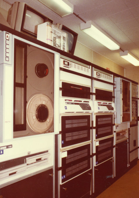
This disk controller controlled an Okidata disk drive at one end and interfaced to the PDP11 Unibus at the other. They consisted of five PCBs (Printed Circuit Boards) as seen in the controller photograph above, housed in the processor boxes in the transaction processors photograph further up. Disk controllers were usually a peripheral which was installed close to the processor as they were susceptible to bus latency and as the bus grant lines were daisy chained, devices closer to the processor were higher in priority. "A" system in the fault log identifies one of the two identical transaction processor racks of equipment A and B. The A and B racks are the second and third racks in the transaction processors photograph above. RTZ is a disk operation command Return To Zero that results in positioning the heads over the power up initialised track.
Interface board Serial Number 467 failing test 0 subtest 0 - incorrect control and status register initialisation. Expected data - 100200 Actual data - 010200. Controller clear command issued from the console would clear bit 12. Any data deposited in any of the controllers registers would result in bit 12 being set. Replaced bus transceiver A3. Now OK.
The Phoenix Disk Controllers were device level interfaces that were used to control the Okidata Disk Drives. These were not like the drives of today you hold in your palm, it was advisable to have four hands to lift them if you wanted to be certain of remaining hernia free. They can also be seen installed with their front covers on at the top of the second and third racks in the transaction processors photo above. Disk storage capacity has increased over the years, it would take about 6,000 of these old drives to match one of today's which can be held in the palm of your hand.
Postscript:
It is interesting to note that I have referred to this again elsewhere on this site and come up with a different figure for the number of old drives to equal the capacity of a modern palm sized disk. I attribute this difference to the influence of Moore's Law as disk capacities have increased over the many years since this was written. The conclusion is that I need a time stamp for the comparison. As I cannot recall exactly when this calculation was made I will provide the new calculation and a timestamp for that. The new calculation revealed 41,944 old 50 MB drives to equal the capacity of a palm size disk drive in 2010.They used the Modified Frequency Modulation method of recording, had a packing density of 5600 bits per inch, had 678 data tracks per surface, 8 heads and 3 platters maximum seek time 75 Msec average 38 Msec. The size was 7 X 22 X 19 inches weighing 65 Lbs. There were equivalent drives at the time the size of washing machines. Additionally unlike the drives of today equipment used to come with large manuals containing circuit diagrams, technical descriptions, circuit alignment procedures, troubleshooting guide and installation instructions. The Okidata manual had about 215 pages excluding the circuit diagrams, which were the fold-out type. These manuals often had suggested component part stock numbers that customers doing their own maintenance should keep on hand for repairs to the equipment. The Okidata manual had 7 pages of suggested parts and quantity based on number of drives being supported from 1 to 1,000 up. These suggested stocks were mainly integrated circuits, resistors, transistors and diodes. Then you had the Phoenix Disk controller to complete the disk mass storage subsystem. It too came with two manuals. The first contained technical descriptions, drawings and programming information like register names and addresses and the meaning of the bits in those registers. The second manual had descriptions of the manufacturer provided diagnostics with assembly language listings.
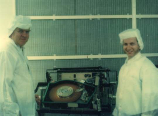
Allan Thomas and I were sent to Goleta in California to investigate and find solutions to the problems ATL were experiencing with these disk drives. Winchester technology disk drives have read-write heads that fly in the boundary layer a few micro inches above the disk platter surfaces. Dust particles appear as major obstacles and result in media defects and head crashes. We were inside a clean room at the manufacturer's premises observing the assembly of the platters, heads, positioner arms and preamplifiers inside the disk enclosures, which are sealed before the drives leave this room. This apparel is required to minimise dust contamination. The wall behind us that looks like corrugated iron, as I recall, is actually part of the air filtration system.
These were an interesting drive as they incorporated a fixed head disk drive as well as a moving head disk drive in the one unit. Drive 0 and drive 1 mentioned in the fault log extract below refer to these drives. The fixed head drive capacity was approximately 2 Mbytes. As I recall we used to install the dividend-calculating program from the fixed head drive to speed up this process. RSX11M, the operating system in use had a maximum program main memory allocation of 32KB and implemented overlays for programs in excess of this size. This required a limited set of modules in main memory at any time and these were swapped in and out as required for execution. The fixed head disk drive sped up this swapping operation, as there was no seek delays in accessing data.
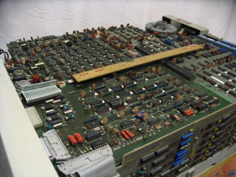
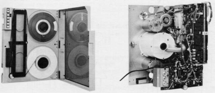
The vertical board bottom right of the photograph is the fixed head amplifier. The horizontal board below the ruler nearest the front of the drive on the left hand side is the data board and the board above this nearest the front is the servo / logic board. The board running the whole width of the two previous boards and towards the rear of the drive on the right hand side is the interface board. The connectors at the rear of this board near the right hand top of the photograph were used to connect to the Phoenix disk controller. Visible at the left rear of the drive is the top of the spindle drive motor, which connects to the spindle via a heavy duty drive belt underneath the drive. This spindle turns the disk platters. This drive belt used to emanate a grating noise resulting from vibration whilst accelerating as it used to spin the disk platters up to speed after the drive was turned on. Two boards are not visible mounted vertically at the rear of the drive. These are the Matrix and the Power Amplifier boards. The Power Amplifier Board is visible at the top left in the following photograph. As nothing more is written about the matrix board I will mention that the heads are selected by a diode switching matrix for moving and fixed heads. The same diode switch is used to read and write using the head selected. The drive has some buttons and indicator lights not visible in the photograph. These are attached to the front panel which is the white metal section in the bottom left of the photograph. A grille was made up to cover these buttons after the write protect button was accidentally pushed during a live operation bringing down the associated system.
This image shows an Okidata disk with the top part of the sealed enclosure replaced with transparent perspex to show the disk platter, the head positioner arm, the positioner motor and part of the moving head assembly. Note that this photo has the front panel on the right whilst the previous photo has the front panel on the left. Additionally all of the electronics PCBs except the Servo Board, have been removed from the top to make this enclosure visible. With the power amplifier assembly at the top left of the photo, used to drive the positioner motor and the Servo Board and the Diagnostic Board plugged into the Servo Board via the Interface Board connector, the head positioning system can be viewed in action. The large complimentary symmetry power stage transistors are clearly visible on the power amplifier assembly. Note the heat sink fins of the heat sink attached to this board for cooling these transistors. I have seen very few instances of electronics bursting into flames and this board is one of them. This occurred one day when one of our managers who was a known jinx to this system visited. This event is described in the ATL The Brisbane Project chapter.
Fault log extracts:
Failing test 6 of the diagnostic disk drive ready bit not set in the disk status register. The problem is in the I/O board. Drive 0 would not respond to any commands. Drive 1 had disk drive ready bit set. U52 not detecting the valid comparison of U50 binary weighted unit select lines and U51 unit select jumper. Replaced U52. Now OK.
Postscript:- "I/O" - the I/O (Input Output) or Interface Board is visible in the image above as identified in the paragraph below it.
 Go back to the index Go to the bottom of the page
Julius Van Disk Serial Number 189. "A" System had drive fault during Albion Park meeting 31/3/79. Hard seek error on running diagnostics. Q9 Power amplifier board emitter leg burnt off and track burnt, R19 burnt. Replaced R19. Rewired new Q9.
Postscript:-
As the word burnt is used in this fault log I will mention that we had a fault on one of these boards that resulted in it bursting into flames. "Julius" identifies one of the two mobile semi trailers that were home to these computer totes, the other was called Premier. These are historical names, Julius from George Julius and Premier the name George gave to his totalisator product in the early 1900s. The power amplifier board contained the electronics that drove the moving head motor to position the heads over the requested track. Q9 is one of the power stage transistors. R19 is a Resistor.
Serial Number 146. Will not read or write. Fault on Data board. Rounded output of U8 causing spurious zero crossing detector to miss transitions. Also RP1 Pin 8 open circuit. Replaced U8 and jumpered U8 pin 9 to RP1 pin 4.
Postscript:-
RP1 is Resistor Pack 1. This is one of my favourite pieces of electronics. It is in the phase locked loop associated with the reading of data from the heads. There was some ECL (Emitter Coupled Logic) ICs in this circuitry and this was my only exposure to this logic family. The transistors in this logic family neither saturate nor completely turn off giving its characteristic of being fast.
"A" disk has experienced a few hard seek errors:- Performed complete servo alignment. Found access time and velocity loop gain were far out of adjustment.
Postscript:-
The servo referred to is the head positioning servo the electronics of which had six adjustment potentiometers that were used to optimise the head positioner acceleration and deceleration profile and track holding capability. I had a science teacher once who told me there was no such thing as deceleration only positive and negative acceleration. What the hell! It was a long time ago and everyone knows what it means! This servo system had two modes. First was "coarse" or velocity feedback mode for moving the heads between tracks and second was "detent" or position feedback mode for keeping the heads above the data track. Both these modes used pre-recorded servo tracks on a platter surface dedicated to the servo. The adjustments were for Servo AGC (Automatic Gain Control), Voltage Controlled Oscillator limit, Up To Speed, Access Time, Velocity Loop Gain and Servo Offset. These were on the Servo / Logic board visible in the photograph above as identified in the paragraph below it.
B disk does not Verify and PIP crashes the system. Ran Phoenix diagnostic. Sector and head address compare errors all over the disk. Ran Supoki to reformat:- diagnostics ran OK. Found new bad block, DUSH = 1437, DCYL = 210. Manually entered this new bad block in bad block file with DSC.
Postscript:-
"Verify" is a disk file structure verification program. "PIP" is the RSX11M Peripheral Interchange Program used for manipulating files. "Sector and head address compare errors" are a result of a mismatch between what sector the disk controller requested and what the disk hardware read from the sector header on the media which contains the sector's address as a means of detecting faults with the head positioning and sector retrieval systems. Supoki - a contraction of Super Okidata, is a disk utility come diagnostic we wrote specifically for this drive. We found that we had written so many machine code programs as a result of having repaired many drives and written tests to decrease time to repair. These were not available with the supplied diagnostics. We incorporated all of the tests into one diagnostic written this time in assembler because of the size of the program and as these routines were used so often it was quicker to run the diagnostic from a floppy disk rather than toggling the machine code programs into memory every time. Having mentioned floppy disks, they are in the process of disappearing altogether, however for those of you who remember them, these were not the 3.5-inch or the earlier 5.25-inch floppies common with PCs, these were 11 inch floppies! A dual RX01 floppy disk drive can be seen in the transaction processors photograph above, located underneath the magnetic tape drive in the first rack. The right hand floppy drive has the access door open. Supoki - after an upgrade in the packing density of the Okidata drives, Supoki was the only means we had of reformatting these disk drives. Reformatting rewrote all the sector and cylinder addresses in the sector headers. DUSH and DCYL are disk controller registers. From memory Disk Unit Sector Head register and Disk Cylinder address register. DSC is a Disk Save and Compress utility, which amongst other things allowed maintenance of the bad block file. The system used this to avoid using bad blocks on the disk media. Later disk drives had media defects recorded on a specially allocated part of the disk media. Later drives still, had hardware capabilities to dynamically reallocate newly found bad blocks to good blocks using a bad block replacement table recorded on the media.
"B" system stopped during EOD at Albion Park. On arrival at the Gabba it was found that the "B" disc would not come ready. Found that UTS (Up To Speed) signal not correct. Looked at NOT OVTEM (not overtemperature). This signal derived from U33 and has NOT SYSRST and NOT OVRCURR plus the thermal switch constituting it. Thermal switch OK. NOT "SYSRST" seemed OK but NOT OVRCURR not correct. This led to the Power Amplifier board. On the power amp board it was found that the centre rail "TP3" was permanently at -32V. This immediately made the two darlingtons suspect. Removed Power Amp board and found 2N6287 to be open circuit. Replaced it and reinstalled Power Amp board. On power up, spindle motor did not even start up. Found F2 blown. Tried another 2A fuse and it blew as well. The first was a fast blow. According to the diagram a 2A slow blow is required. Put in a slow blow and now running OK.
Postscript:-
EOD - End Of Day procedure. Albion Park and the Gabba two tracks were the van went to provide totalisator services. NOT SYSRST, NOT OVTEM and NOT OVRCURR are signal names NOT SYStem ReSeT, NOT OVer TEMperature and NOT OVeR CURRent. I have changed the name of these signals as they are written, to include the NOT in front of them. They are written without the NOT but with a bar over the top of the characters in the name indicating the not condition. These signals are all part of the error detection logic and exist in the Servo / Logic board. The Power Amplifier board mentioned uses complimentary Darlington power transistors biased so that only one can conduct at a time when driving the positioner motor. Darlingtons are two cascaded transistors in one package giving a high current gain. The two Darlingtons mentioned, were a complimentary symmetry pair, one PNP the other NPN. The first pulls the centre rail, mentioned in the log, up and the other pulls the centre rail down in voltage, as required. F2 is a fuse. 2N6287 is a Darlington PNP transistor. Fast blow fuses blow quickly after reaching the limit current, slow blows will allow short excursions above the limit current without blowing.
"A" MT failing diagnostics. Found that after any data transfer command controller never came ready. Wrote program to write to the MT, delay, then check if CUR set. If not issue a Power clear command, rewind and try writing again. Controller signals to tape ISFC and ISWS were correct. Controller waiting for EOF sequence from MT. Determined that MT write signals TP102-TP903 of write card were correct. On examining read signals found channel 5 read amplifier TP701 oscillating. (DATA K-1 BOARD) Replaced U8 on this board. Now OK.
Postscript:-
These tape drives are visible below and in the first and fourth racks in the transaction processors photograph above. The controllers for these drives were Western Peripherals Model TC-130/138 Tape Controllers which were implemented in 4 PCBs housed in the expansion boxes immediately below the processors visible in the previously mentioned photograph. MT is a mnemonic for Magnetic Tape drive. CUR is Control Unit Ready bit in the command register that signals readiness to accept a command. ISFC and ISWS are acronyms describing electronic signals sent from the tape controller to the drive that stand for Inverted Synchronous Forward Command and Inverted Set Write Status. The names have inverted as a prefix indicating that these signals are active low rather than the more common active high. The EOF is End Of File. TP is Test Point. U8 is an Integrated Circuit identifier. The program written for this problem would have been a machine code program like the one mentioned at the top of this page.
Computer hardware in those days really contained some serious metalwork. These magnetic storage tape drives weighed 155 lbs and for the metric generation 52.16kg. The inertia of the tape reels required large motors to drive them. Despite these heavy motors, vacuum columns visible to the left of the reels were required to buffer the tape as the reel motors could not accelerate and stop as quickly as the capstan, which controlled tape movement. The vacuum columns also provided the means for the reel servos to adjust the reel's angular velocity dependant on the amount of tape on the reel to provide a constant tape velocity.These tape drives were hinged and they could be swung out from the rack creating an arc behind them which you could squeeze into to gain access to the drive's large printed circuit boards for maintenance. One day I was analysing a problem with one of these drives. I was squeezed in this arc with an outstretched arm placing a CRO probe on pertinent points in the circuitry related to the fault symptoms. The branch manager, who had an engineering background, noticed that I seemed more contorted than appeared necessary and he asked why. I replied that my upper arm was close to the 240V section of the drive and I was ensuring that I do not touch any part of this to avoid an electric shock. He asked if I did not like electrical shocks. I replied that I did not. He then said I suppose you do not check for the presence of 240 volts by tapping your fingers on the live terminals. I confirmed that this was the case and that I used a meter for determining the presence of 240V. His reply was why not it's just a little tingle up your arm. I considered this conversation to be techno-humour however I could not escape imagining him actually testing 240V this way. Nowadays, the Workplace Health and Safety staff would take a rather dim view of such a suggestion.
While copying files with BRU from the M.T. to the disk for the VOTS system, BRU encountered parity errors. Ran Diagnostic WPDI34 on the Mag Tape, Errors logged :-
| PC | Status | Command | Byte | CA | DATAB | READL | TEMP | CRCCAL |
|---|---|---|---|---|---|---|---|---|
| 3552 | 10101 | 160206 | 177777 | 14556 | 0 | 1000 | 0 | 0 |
| 4040 | 110 | 60210 | 0 | 14722 | 0 | 101000 | 0 | 0 |
| 4050 | 101 | 60210 | 0 | 14722 | 0 | 1000 | 0 | 0 |
Much more was printed following these lines. The first failing test wrote an EOF mark and encountered a parity error reading it. Scope looped on this test, however it was useless for testing all data channels due to the dead tracks in the EOF mark. Wrote a programme to write single bytes on the Tape. Examined the write channels with a CRO - all OK. Examined the read data channels and found read data missing on channel 2 at TP403 and 404 on Data K1 board. Further investigation found read data on TP401 but not TP402. Examined U15-A pin 5 and found read data present. As an Op Amp in linear application has Vd=0 deduced that U15-A was faulty. Replaced U15-A. Now OK.
Postscript:-
BRU is Backup and Restore Utility. VOTS - Victorian On-course Totalisator System, we were upgrading the Brisbane system with improvements incorporated in VOTS. PC is Program Counter containing the address of the test where the error occurred. STATUS is the contents of the controller status register at the time of the error. COMMAND is the contents of the controller command register at the time of the error. BYTE is the contents of the controller byte counter at the time of the error. CA is the contents of the controller current memory address register at the time of the error. DATA B is the contents of the controller data buffer register at the time of the error. READ L is the contents of the controller Read Lines register at the time of the error. CRC CAL is the calculated CRC character which is only significant for the CRC test. CRC is a Cyclic Redundancy Check used for data error detection. From memory these drives had 9 channels recording 8 data bits and one parity bit for every byte recorded. This parity bit constituted lateral error detection. The CRC was appended to blocks of data and constituted a longitudinal error check. Scope looped - the diagnostics could use switch register settings that they often examined at address 777570 to alter their behaviour. In this case by setting bit 14 in the switch register it was possible to get a particular test to enter a tight loop suitable for generating signals for analysis with a CRO. EOF - End Of File. Op Amp - Operational Amplifier in an integrated circuit. Vd=0 differential voltage across the input legs of an operational amplifier is ideally 0 when used in a linear application.
Julius van - Could not load tape. Unable to adjust -10V regulator. Found Q16 blown. Replaced Q16 and adjusted -10V OK. To get tape to load had to adjust SUS and TUS fully clockwise and ramp supply and takeup reel servo pots fully counter clockwise. Now does not sense BOT. Tape sensing lights are out. Manipulated J504 and sense lights came on. Cleaned up J504. Aligned SUS TUS and supply and takeup ramps. Ran diagnostics - all OK.
Postscript:-
Q16 is a transistor. SUS and TUS - SUpply Speed and Take Up Speed potentiometers controlling supply and takeup reel motor speeds by providing adjustable tachometer velocity control. BOT - Beginning Of Tape, which is marked with a reflective silver tab stuck to the tape with sufficient leader to allow for the distance between the reels and the amount of tape in the vacuum columns. This ensured that sufficient tape remained on the takeup reel so you did not run all the tape off the reel when rewinding. It also was the point after which data recording started. The "sensing lights" reflected from the silver tab triggering a sensor. J504 is a connector. The ramps mentioned are electronic waveforms for the takeup and supply reel servos which control the servo response to the capstan speed information as switched by the vacuum switches. The vacuum switches sense where the supply and takeup loop of tape is in the supply and takeup vacuum columns.
After entering $DB (trying to boot) ***EXEC PARITY ERROR*** printed. Quick DZKMAC on 0-64K showed bank 6 as having a parity error. A quick run of DZKMAC without parity gave us the locations, which were within bank6 and also the good and bad data. This showed that bit4 was consistently inverted. By checking the arrangement of the RAMs Z34 appeared to be the offender. Replaced it and all okay.
Postscript :-
MOS refers to the Metal Oxide Semiconductor logic family used to implement this main memory. This memory was stored in the processor box. DB is a disk drive specifier used to start a bootstrap operation. DZKMAC is a main memory diagnostic. Parity is an error detection method which is implemented with a single bit which is set to make the total number of bits it is checking and itself an even number or an odd number depending on whether even or odd parity is being used. It is stored with every byte written and checked during read operations. Twenty two years ago and when I read these logs I still can relate the writing to the names and faces. This was highly competent Laurence. He went to IBM.
Postscript :-
Shared memory was a core memory which was dual ported and could be accessed by two computers. There was no network linking the master and slave computers in this hot standby implementation. This shared memory was the means of interprocessor communications. The PCBs comprising this memory were housed in the bottom expansion box in the second and third racks in the transaction processors photograph above. The lower shared memory was in the second rack and the upper in the third rack. There was an interesting problem synchronising access by the two transaction processors to this memory. A flag, a single bit, was used to indicate when one of the transaction processors was updating this memory to lock the other one out until completed. Some machine code instructions were used to manipulate the flag however as the processor released the bus during instruction execution it was possible on very rare occasions for both processors to gain modify access to this shared memory at the same time if they both executed the flag manipulating instruction at the same time. It was found that an ASL Arithmetic Shift Left instruction performed the read and modify operation on this flag without releasing the bus between these operations and the ASL was used to resolve this problem.
Upper shared memory failed DZKMAC diagnostic, which reported dual addressing errors.
| Location | Good | Bad | PC | Error | PASFLG |
|---|---|---|---|---|---|
| 577772 | 117772 | 117776 | 2664 | 23 | 0 |
| 577762 | 117762 | 117766 | 2664 | 23 | 0 |
| 577752 | 117752 | 117756 | 2664 | 23 | 0 |
| 577742 | 117742 | 117746 | 2664 | 23 | 0 |
| 577732 | 117732 | 117736 | 2664 | 23 | 0 |
Set up memory management registers to relocate console accesses through console emulator to upper shared memory and deposited data in upper shared memory using the console emulator.
| Location | Deposited | Examined | Faulty |
|---|---|---|---|
| 0 | 0 | 0 | N |
| 2 | 1 | 3 | Y |
| 4 | 2 | 2 | N |
| 6 | 3 | 3 | N |
| 10 | 4 | 4 | N |
| 12 | 5 | 7 | Y |
| 14 | 6 | 6 | N |
| 16 | 7 | 7 | N |
| 20 | 10 | 10 | N |
| 22 | 11 | 13 | Y |
| 24 | 12 | 12 | N |
| 26 | 13 | 13 | N |
| 30 | 14 | 14 | N |
| 32 | 15 | 17 | Y |
| 34 | 16 | 16 | N |
| 36 | 17 | 17 | N |
| 40 | 20 | 20 | N |
Data bit 2 changed whenever bit 1 was set.
Wrote a routine to continually access one of the faulty addresses above in shared memory. Found E18 pin 8 of Unibus interface board being decoded correctly, however pin 8 of E19 was incorrect when displayed on the CRO, with respect to pin 10 of E5 (BANK00 SELECT H). E17 pin 8 was causing E19 pin 8 to be disabled while this stack was selected.
E17 pin 10 correctly disabled "and gate" (pins 9&10) however Bank 01 (02,03) select H had 2V pulses present.
Inverters E5 pins 3&4, 5&6, 8&9 should have driven these signals (BANK01 SELECT H, BANK02 SELECT H, BANK03 SELECT H) permanently low, from their input signals, which were held high by pull up resistors R25, R27 and R28. Replaced E5. Memory now OK.
Postscript:-
The routine mentioned above will have been a machine code program like the one mentioned at the beginning of this page. The headings in the first table are LOCATION failing memory location, GOOD the data that was expected, BAD the data that was found, PC the Program Counter at the error call, ERROR the failing error number and PASFLG is the contents of location PASFLG which is not relevant to every test. Error 23 is a Dual Addressing Error, if PASFLG=0 then the failing location and failing data ae dual addresses.
Postscript:-
The DMX11 in this system was a purpose built multiplexer by Digital Equipment Corporation's Special Systems Group. It predates the DMX mentioned in the machine code section above which was implemented as a separate device to the transaction processor. This DMX interfaced to the transaction processor's PDP11 Unibus and occupied several backplane slots. The PCBs comprising this multiplexer were in the expansion boxes below the processors in the second and third racks in the transaction processors photograph above. At the bottom of these racks are two blank covers. They could be pulled down to expose the TIM (Ticket Issuing Machine) line patch panel. These accommodated 32 TIM lines capable of supporting 16 TIMs on each. This multiplexer was capable of handling 64 lines however 32 was sufficient for our needs. The patch panel incorporated RS232 to Differential and Differential to RS232 converters along with protection diodes for each line. The RS232 side connected to the DMX. The tri-state differential lines ran relatively long distances around the tracks to connect to the ticket issuing machines. The Brisbane department ended up repairing these DMXs for the whole company. The DMX had two levels of PDP11 diagnostics. One diagnostic could analyse some faults utilising the tote firmware in the DMX. Another was used for in-depth fault analysis requiring the DMX firmware to be changed to accommodate this second diagnostic that ran in the host PDP11. Some of the DMXs sent to us for repair had multiple problems as evidenced in the following log entry. This example also demonstrates how you can end up going in circles as a broken track is repaired only to find that it was a valid modification and had to be undone.
Plugged the DMX into the maintenance system. Responds to Unibus address OK but does not run internal loop-back test. This diagnostic reports line unit processor timeout errors E#15 on every line. Installed diagnostic ROM in USART board and ran Z04UE diagnostic. It failed test #1 subtest #1 E#2 GOOD:0 BAD:302 DATA:27101 GROUP#0. Using test number 3 was able to determine through "write" and "view" commands that a few RAM locations were faulty in the range 20000 to 20400. Locations from 20400 to 27000 were all OK. Found that RAMs E82 and E67 of drawing D11 USART Module were being selected through E96 even while no diagnostic access to these locations was being made. Traced this to a faulty address decoding IC E74 drawing D2 of USART Module. The address input A0 to A2 never selected MEM1L. Replaced E74. Diagnostic now passes subtest 1 OK.
Track at top of right hand corner of USART E42 broken. Does not appear to have been a modification - reconnected it.
2/10/84 ZOVUE now fails Test #1 Subtest #2 ERR#5 DATA=177463 GROUP No 0. This error occurs if the line unit transmit silo did not reset. 177463 is the address of the TX Silo control register D2 of USART DMX drawing I/O address assignment 177463 - 177400 (start addrs of I/O page) = 638 (3316). This register is described in the DMX technical description manual P4-12
| DB7 | DB6 | DB5 | DB4 | DB3 | DB2 | DB1 | DB0 |
|---|---|---|---|---|---|---|---|
| TX RDY | <---- | TX Line | Number | ---> | TX RESET |
This register is at the top right hand corner of D7 USART Module Engineering Drawings. Setting bit 0 in this address using test 3 of Z04UE diagnostic should have reset E123. (i.e.TXRDY) but it did not. Setting test 3 up to continuously set bit 0 in this register, was able to determine that E29/32 would set E123 again after it was reset. This was due to input pins 16 and 20 being active on E29. Traced this back through E10 and E14 and found signals "TXRDY09H", "NDTR09H", "TXRDY13H" "NDTR13H" all at 2V. Replaced USARTS E3 and E7. Diagnostic now passes Test #1 Subtest #2 OK.
3/10/84 Now failing TST#1 Subtest #3
E#20 DATA:4 GROUP No 0 Called From 4572
E#22 GOOD 252 BAD 0 DATA:4
E#20 DATA:5 GROUP No 0
E#22 GOOD 252 BAD 373 DATA:5
E#20 DATA:6
E#22 GOOD 252 BAD 377 DATA:6
E#16 DATA:7
E#20 DATA:7
E#22 GOOD 252 BAD 0 DATA:7
Rest of test OK.
i.e. UARTs 4,5,6,7 found faulty by diagnostic. These are E42,E43, E44 and E45 respectively. These comprise group 1. Found group 1 CLKL switching from 2V to 4V. Found pin5 E11 (Drawing D9 USART module) OK. Pin 6 faulty. Replaced E11 - still the same. Traced the tracks involved in a modification in this area and found that the track repaired 2 pages earlier should have been open circuit. Open circuited this track again and Group 1 CLKL now OK.
Now failing Test #1 Subtest #1 again. E74 Drawing D2 USART Module is decoding accesses to all memory mem0 to mem7. Using test 3 it is not possible to modify RAM. Looks like the Line Unit Processor is writing continuously to RAM. Changed 2A-H04UA ROM (diagnostic ROM) - now RAM OK.
Z04UE now failing Subtests 3&4
Test No1 Subtest#3
E#22 GOOD 252 BAD 2 DATA:7 Group No 0
Test No1 Subtest#4
E#46 GOOD 2 BAD 0 DATA:7 Group No 0
i.e. USART number 7 Faulty - table top right hand corner of Drawing D2 USART MODULE USART7 -> 01EH SELECT -> Drawing D8 SELECT01EL -> E35 -> USART E45. Replaced E45. Z04UE Test #1 now passes all 6 subtests.
Note: Switch Register settings used for Z04UE were
4 110 tst1 subtest 0 on Group 0
4 130 test3
Replaced Tote firmware in USART board and ran Internal Loopback test - All OK.
Solution BLTs do not function at all. Lower data bus bits 0-7 has collapsed, operating between 0 and 0.5 volts. Bits 0 through 3 had a mutual resistance measurement < 1Kohm. Removed components from the bus until low resistance disappeared. Problem was status register A U101. Replaced same. TIM now runs all BLTs according to the 7-segment display. There is still no operator display function. Replaced 2-bit stripper PAL U416 now ok.
Postscript :- BLTs are Board Level Tests inbuilt to the TIM firmware and were selected by setting a switch in a switch pack. There was another level of tests above these called BATs, which were Basic Assurance Tests.
Fault Blank Operator Display.
Solution This TIM has been out of action in excess of 8 months. It was initially diagnosed by someone else who ordered a video RAM. As the video RAM has been on order for 8 months I replaced it with one from another board. This did not cure the problem. The diagnostic display showed a "TRAM" error in the TP01 diagnostic, which is a "Destructive RAM test failure on video memory". Found no data on the Font RAM data bus U401 pins 11-13 and 15-19. This was due to a very distorted signal at U407 pin 19 OE*. Postscript:- OE* a signal called Output Enable Low. Found an open circuit between this pin and U414 pin 3. Repaired same and tested OK. Also had to replace U416, the CCD reader and several keycaps, which had been pinched for other machines. Also a faulty operator display had to be installed. These have been on order since June and the one from this TIM had been pinched to get another TIM working. The faulty operator display has a vertical line through the display area however it is still usable.
Solution The display showed the correct data, however the bottom 3 pixels of each character were reproduced where it's top 3 pixels should have been. U415pin7 (F2A2, output to font RAM) was permanently low. Replaced same. Postscript:- The time logged on this fault was 15 hours.
Fault If $AMT and 1 keys are simultaneously pressed First 4 is displayed.
Solution Found that this applied to all the keys in this column. The Keyboard modification had not been done as per document MISC57 BC:SM 27/10/92. Performed keyboard modification and tested OK.
Solution Found CN400 pin 12 MD1 data from the 2-bit stripper at a much higher rate than normal. Traced this back to an open circuit between U416 pin 16 and U420 pin 5. After removing the board and examining U420 closely found a green powder like material around pins 5 and 6 of U420. Copper Oxide? The open circuit was underneath the IC on the top side of the board so it was impossible to examine it closely without removing the IC. Cleaned the green powder off and soldered a piece of wire to replace the broken track. Ran diagnostics OK.
Solution Appears that coke has been spilt into the printer causing Q6 Q11 R50 and VR3 to fail. Replaced same.
Solution Found that the network port transmit & receive IC's (DS3695) were both faulty. Replaced & ran diagnostics OK.
Solution The network port ICs had failed again. Noticed that this board had no transorbs or protection diodes. They had been cut out! Installed transorbs and replaced network port ICs again. Performed down line load the comms loading. 1400 messages @ 210 bytes OK. Then performed power reset to see if transceivers survive. Then 2470 messages at 200 bytes OK.
Postscript:- "MJ" mentioned above is a term we applied to a process of removing connectors and possibly all plug-in components cleaning contacts and replacing them. It acquired the name Mumbo Jumbo as it became significant, ending up rectifying about 80% of faults and lacked any analysis whatsoever.
Solution Replaced U14/LT1081 interface IC
Postscript:- This sort of fault is a nightmare on raceday! Up to 16 machines out of action.
I recall this fault very well. The solution here starts after work had been done where this TIM was in use at Caloundra. This is an example of the obscure type of symptoms network problems can produce. After a long standing problem there escalated from tolerable to a definite nuisance level we went up there to have a good look at the LAN. On measuring the LAN there was an unusually low resistance across a couple of the conductors. This was a tri-state differential line. The cause was isolated to this machine. The reason this problem had been unresolved for so long is that this machine regularly caused symptoms to be experienced on other machines on racedays.Fault TIM has 5 ohm resistance across pins 1 and 2 of the network port connector causing obscure LAN problems. Curiously this has not stopped this TIM from functioning. Problems have existed on the Caloundra office 415 NetMan93 LAN for a couple of years. The master always stays on line and slaves drop off individually sometimes alternating on and off line. The problem usually starts at seat 9 and others follow. The seats affected are 1,3,5,7,9 and 11. This TIM was in the seat 5 position.
Solution Replaced U500. The low resistance was across pins 6 and 7 of this IC. Also cleaned out an insect nest between the left hand ends of R501 and R500.
Postscript:-
We often had insect colonies set up inside equipment. One TIM91 console was found with so many ants in it that I opened it up and placed it somewhere for the ants to exit to reduce the population before starting to clean it up. On this subject, the worst task I had was to clean up a TIM91 that had been subjected to a shower of sewerage at a trotting track where plumbing work in the ceiling went awry.
Solution Battery volts down to 2.5V, replaced battery
Solution Inherited this PCB as hard to fix. Found RV2 was 500 instead of 1K Ohms. Replaced with correct value. Also Q10 and Q21 had been replaced with a transistor that had the base on the right hand leg instead of the centre. The replacements were BC182Ls instead of BC182. Could not source BC182s so twisted legs of the BC182Ls to fit in the right holes. LK1 is now at 20V and is adjustable. Still does not print. Found the printer strobe oscillator output at TP6 had a period of over 10 microseconds instead of 2 microseconds. It was not adjustable to within limits with RV4. Found an open circuit track between U9 pin 6 and C53. Bypassed faulty track, adjusted RV4 for 2 microseconds at TP6 and tested printer OK. *************** For future reference noticed that U6 pin 10 has part of the socket pin hanging out. As it is working at the moment have left it this way.
Solution Found that it does not run TH12 BLT. It does not complete this test but resets before the OK status. Suspecting that the processor is hanging and that the watchdog timer was causing the reset removed pin 15 of U102 MRESET* from it's socket. As suspected we now hang in TH12. In this static hang state found DMA request signal REQ1* pin 26 of the 85230 asserted. Found WACK1 pin 20 of PAL U706 missing during the DMA transfer. Replaced U706 and TH12 worked OK. Examining the removed IC found pin 13 pressed flat across the bottom of the IC which means it had not been in contact with the socket. Straightened the pin and reinserted this PAL. TH12 now ok with original PAL.
Postscript:- DMA is Direct Memory Access. A means for peripherals to transfer data directly to main memory without needing assistance from the processor. REQ1* and WACK1 are request and acknowledge signals associated with the DMA. The * after a signal name indicates that it is active when low.
Solution Failed asynchronous host loop back test and BLT ts02. Further reported error "thrt" suggesting problem with RTS/CTS path, sync clock or DMA circuit. Found open circuit between pin 4 (RTS) on host port and pin 6 on IC U503. Repaired same and passed BLT's
Postscript:- A loopback test loops the transmit line to the receive line so a diagnostic can determine whether the transmitted data is the same as what it sent. RTS is Request To Send and CTS is Clear To Send.
Solution Fails TH12 BLT. If run BLT in asynch mode ( see maint.txt ) then ok. Found TH12 failing by hanging during a DMA transfer which is used for synchronous comms. Found pin 27 of U506 the SCC and pin 12 of U200 the processor, not making contact with the socket contacts. Amazingly these are two ends of the same connection REQ1*. Resprung contacts on sockets. TH12 ok.
Postscript:- Serial line communications can be synchronous, requiring a separate clock to synchronise the receiver with the transmitter or asynchronous (asynch) requiring embedded start and stop bits to achieve synchronisation.
Solution Could not replicate fault as machine would not respond. Cleaned keyboard and then found key "0" would decode as "3" and also trigger keys "1","4","7","2" and "admin" Removed, cleaned and replaced keyboard controller BB68 and machine operated correctly on-line, passing all BAT's and terminal maintenance tests.
Solution Found A2 bus line broken between the PCDC and the 7-segment Display. Repaired this and the 7-segment display now shows K--m consistently. Compounded problem! This consistent K code obviously means something however we do not have any documentation on it. Asked Van Thai for a copy of the BAT diagnostic code. Further investigation showed that none of the I/O devices were being written to, IOWR* control line never asserted. This was traced back through a PAL to the processor pin 23 RW*. When this was monitored with the CRO at the PAL this signal was a constant high. When pin 23 was probed at the processor end the tim started to work. This pin was found pushed back in the socket. Removed the processor and used a very fine piece of wire to pull the pin back out. Reassembled tim. Replaced RAM expansion board. RAN all BLTs and maintenance tests. All OK.
Postscript:- The 7-segment display is a diagnostic display. This is a case where the diagnostic tool had to be repaired before the fault could be attended to. I have also seen the situation described here on many occasions where a circuit starts to work as a result of placing the CRO probe on a particular component leg.
Of course all this work had to be performed somewhere. This photograph shows half of the maintenance area at Eagle Farm Racecourse.
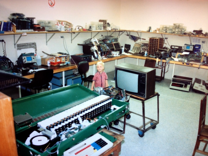
Although we had facilities to perform simple repairs at each of the tracks, this is where all the serious problems were rectified. This photo was taken during the VAX based tote era. The blue devices under the left hand bench are J25 TIMs and the terminals below the right hand part of the bench are J22 TIMs. Three CROs are visible, the Tektronix 465s are visible at each end of the bench and the one in the middle of the benches, in the far corner of the room, is probably the Hitachi. The green device in the foreground is a BET3400 Bookmakers Terminal ATL manufactured.
The smiling face in the middle of the image belongs to Ian Conlon. At the age of 11 he assisted with writing the HTML for this website. He later attained an Information Technology Degree from QUT and whilst a student provided part time assistance on the race tracks preparing for large meetings. His first permanent job was at the racetrack as a Raceday Manager where he was also heavily involved in Hardware and Software engineering. From there he progressed to working for a start-up Telco called Indigo Telecom as a Network Administrator. He further progressed to working for Shine Lawyers as a Business Analyst in 2013. This area in the Old Main Tote house looks very different now in 2013, being part of a magnificent function room called The Tote.

| Previous page | Go to the index | Top of the page | Next page |