This technology history page contains a photograph, which is one of several belonging to the photo gallery pages, which are part of several pages relating to the invention of the world's first automatic totalizator in 1913 and Automatic Totalisators Limited, the Australian company founded in 1917 by George Julius to develop manufacture and export these systems.
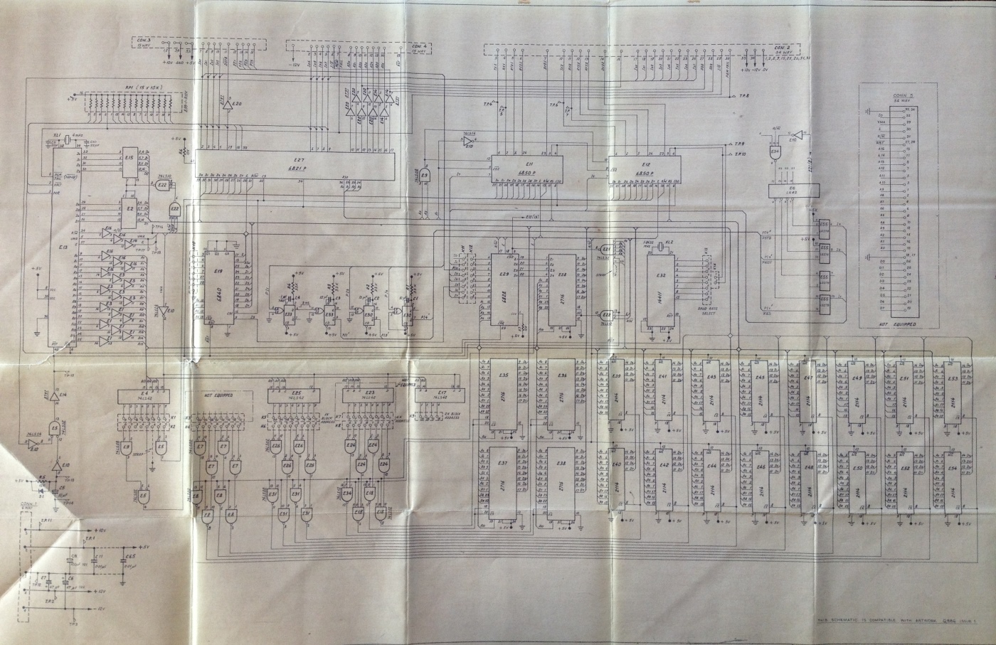
J22 Processor PCB Circuit Diagram
This is an image of the J22 Processor PCB (Printed Circuit Board) Circuit Diagram extracted from the J22 Technical Manual. As with the block diagram of the J22 in the previous image of the Photo Gallery, I have deliberately not made much effort to straighten out the folds in this diagram to demonstrate how it unfolds from the manual. In the interests of clarity of the text in the diagram, I have not shown a wider view as in the third image below, so it does not show the rest of the manual to which it belongs. This circuit diagram shows the electrical components and connections on the Processor PCB, which is shown as a block in the Block Diagram in the third image below. The Block Diagram shows how each of the modules connects with all the other modules in the J22. More after the image...
Click on the image to go back to the photo gallery
Photo by Brian Conlon
An Overview
The J22 Technical Manual Part 2, which contains the drawing above, was published during an era when manuals were in printed form and not distributed on computer media like CDs or DVDs or on the Internet, as is the custom at the time of writing in 2015. I recall a period when it became popular to distribute technical information, Circuit Diagrams, Circuit Descriptions, Diagnostic Listings etc on a medium called Microfiche which greatly reduced storage space. Microfiche was like large negatives, each containing many pages of information and these required a specialised reader which enlarged a single grid referenced page in the negative and presented it on a screen.
The integrated circuit identified as E13, represented as a tall, plank like, vertically oriented oblong rectangle, near the left hand edge in the upper half of the drawing above, is the M6802 Microprocessor. This has previously been referred to in the Photo Gallery, as the M6800 which refers to the architecture that permeates through all of the M6800 IC series. In the J22 TIM image page in the Photo Gallery there is a section that gives an extract from the M6800 firmware as a small example of the program code that is executed and it is this IC labelled E13 that executes that program. This can be read by clicking on the image above and scrolling up two image thumbnails to the thumbnail with associated text starting A retired old workhorse J22 TIM and selecting that thumbnail. Finally scroll down the the heading Sample of the J22 M6800 code.
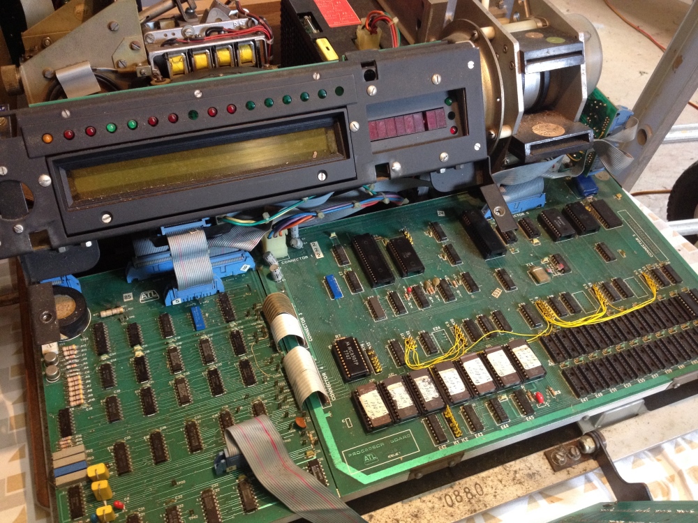
The image below shows a J22 with its covers removed. There are two PCBs clearly visible with three short arched ribbon cables bridging the left and right hand PCBs. At the bottom left hand corner of the right hand PCB, below the bridges, there is a board identification inside a white outline. The words PROCESSOR BOARD and the ATL logo are visible. The drawing above defines the electrical connections of this board. There are five rows of integrated circuits (ICs) in the processor PCB shown in the image below. The top row contains two long ICs. The right hand IC is the M6800 Microprocessor mentioned and identified in the drawing as E13.
Inside the J22 with covers removed
In the bottom right hand corner of the original paper drawing, which is not shown in the image at the top of this page, is a Title Block similar to the one visible in the image below. In this title block, in the Drawn By box are the initials A.A.C and the Date box shows 7.7.78. Neville Mitchell made the following comments about A.A.C:
The design draftsman who drew the Processor circuit was Alex Chitoff. He was hired by me from a contracting company who were syphoning off 14% of his hourly payment. Alex was a wonderful guy not only could he draw digital circuitry he also did the manual precise work, laying out the PCB using detail from the engineers draft and parts lists. In this era, the PCB layout and tracking was done with pre-cut adhesive pads and tapes, all work carried out on light box desk tops, we redesigned these boxes adding a mix of fluorescent and dimmable incandescent lamps, which help with eye strain as twelve hour days were normal.
To my knowledge he never made an error that was his fault. Alex approached me asking for a transfer to my staff, with a substantial pay rise. At the time I could not afford to loose him. The contract company demanded a release fee of $8000. ATL management had a fit but realised the situation we were in, with the development of the J22 running very late. They decided to pay the fee and Alex worked for me for a long time. He was later involved in the J24, J25, J42, terminals and the Mono Rail projects.
Notes on the following extracts from the J22 Technical Manual:
In the following text, which is a technical description of the Processor PCB Circuit Diagram shown at the top of this page, there is an obvious discrepancy in the component designations. I can only think that the circuit diagram I have above is not one of the Brisbane J22 diagrams but possibly belongs to the Hong Kong project. The original diagram from my Brisbane specific manual has been lost. Unfortunately so much time has elapsed since these machines were used, I think there would be next to no hope of finding the correct Processor Circuit Diagram for the Brisbane Project.
Consequently, wherever the Technical Manual description below refers to a circuit component designation, I will provide the corresponding designation in the above diagram in brackets behind the one given in the manual. For instance the M6800 mentioned in the text below is identified as E7 so I will append (E13) to it.
Many ICs have multiples of the same circuit implemented in them. In most cases the digital electronic PCBs on which these ICs are installed will utilise one type of circuit repeatedly and having multiples of one circuit on one IC is a space, complexity of implementation and cost saving method. In the Technical Manual text, where more than one circuit exists, a letter follows the IC circuit designation indicating which particular circuit in the IC is used at that node in the circuit diagram e.g. (E5f). In this case, the designation E5 will appear multiple times in the circuit diagram and to be sure that you are looking at the right place in the circuit relating to the description you either need the following letter specified on the circuit diagram or you need to know which contacts on the IC correspond to the following letter. This requires access to a Data Sheet on that particular IC. As the circuit diagram in the image above does not identify the following letter, I have provided the pin numbers of the IC specified by the circuit designation instead e.g. (E16 pins 2 and 3).
Two obvious differences between the circuit diagram and the Brisbane Project Technical Manual is that the latter indicates capacity for more RAM ICs and EPROM ICs. My memento J22 TIM, shown in the second image below, like the J22 Technical Manual has the increased number of RAM and EPROM sockets. The PCB drawing at the top of this page indicates there are five 2716 EPROMs designated E28 and E35 through E38 and eight pairs of 2114 RAM ICs designated E39 through E54. The inside view of my J22 shown in the image above has seven EPROMs, which are the ICs with white labels on top of them, two more than shown in the drawing. The labels provide dates, version numbers and code segment starting addresses of the EPROMs. The labels have a second function as they keep light from entering the EPROM window as the ultraviolet component is used for erasing the EPROMs and unless they are to be reprogrammed, this is obviously undesirable at any other time. It can be seen that every EPROM socket is occupied. To the right of the EPROM sockets, two banks of RAM sockets are visible, of which there are twelve pairs, providing four more pairs than shown in the drawing. It can be seen that only the first two pairs of RAM sockets on the right hand side are populated with 2114 ICs.
The J22 Block Diagram from the Technical Manual
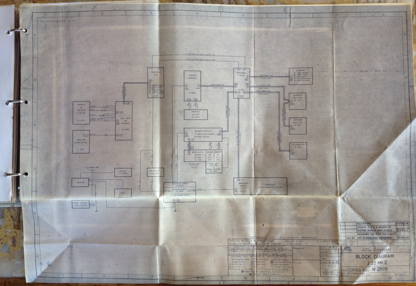
The Block Diagram above shows the outermost view of the TIM, identifying its major functional units or modules. Inside the blocks in the diagram there are drawing numbers that identify the drawings that provide all the details of the module relating to the block. The block diagram shows the whole machine and how the blocks interconnect. The Processor PCB Circuit, as defined in the Diagram at the top of this page, is represented in the above image, by the left hand box in the top row of boxes. There is a larger rendition of the Block Diagram image in the Photo Gallery pages of this website. To view the larger rendition with additional information, click on the image at the top of the page to return to the Photo Gallery, scroll up and select the J22 Block Diagram thumbnail.
3.4 Processor Board Page 3/4
Following is an extract from the J22 Technical Manual part 1 section 3.4 starting at page 3/4. It begins with the text Refer to Figure 3 which is a copy of the Circuit Diagram in the image at the top of this page. The Technical Manual Extract follows:
This board controls the complete operation of the J22 Mark II TIM. The Processor Board has provision for up to 24 internal 1024 X 4-bit Random Access Memories (RAMs) and seven internal 2K X 8-bit Programmable Read Only Memories (PROMS). Only four of the 1024 X 4-bit RAMs are used on the Brisbane and Harold Park Totalisator Systems. The transfer of data and control functions between the Processor and Peripheral Control Boards is via a Peripheral Interface Adaptor, (PIA) and between the Processor Board and the host processor via two Asynchronous Communications Interface Adaptors (ACIAs).
3.4.1 Microprocessor Unit Page 3/5
The Microprocessor Unit (MPU), E7 (E13), receives interrupt requests( IRQ ) from the peripherals, via a Priority Interrupt controller (PIC), E21 (E29), requesting that an interrupt routine be generated. The MPU waits until it completes the current instruction before it recognises the request. The MPU then responds to the request and the PIC directs the MPU to the proper memory location. In addition, a Programmable Timer Module (PTM), E4 (E19), is used to generate system interrupts. The PTM is under MPU software control.
An internal 1 MHz oscillator supplies the two-phase clock pulses to drive the MPU. The oscillator is controlled by an external 4 MHz crystal and an internal divide-by-four circuit. A single-phase TTL compatible clock (E) is used to drive the memory devices and the interface adaptors.
A Reset ( RST ) input from E44d (E14 pin 13) and associated components is used to reset and start the MPU from a power down condition, resulting from a power failure or an initial start-up. When power is applied to the Processor Board, capacitor C5 is charged to +5V via a resistor R5. At a time determined by the time constant of C5 and R5, the Schmitt trigger E45a (E10 output pin 6) is triggered and a logic low is met at its output. This is inverted by E44d (E5 pin 13), buffered by E2e (E14 pin 13) and fed to the RST input of the MPU to initiate the reset and restart. The RST is also used to reset the firmware and other devices in the Processor Board. Provision is also made for the RST input to be triggered from an external source.
The Read/Write ( R/ W ) output from the MPU signals the interface adaptors, memory and other devices that the MPU is either in the READ (logic high) or the WRITE (logic low) state. The output is TTL compatible and is buffered by a hex three-state non-inverting buffer amplifier, E5f (E16 pins 2 and 3).
The 16 bit address, A0 to A15, is used for memory addressing and for peripheral addressing. The address bus outputs are also TTL compatible and are buffered by E5, E6 and E18 (E1, E3 and E16); all buffers are permanently enabled. The valid memory address (VMA) output signals that there is a valid address on the address bus and is used to enable the peripherals and memory devices. This signal is buffered by E2b (E16 pins 4 and 5).
An 8-bit bi-directional data bus, D0 to D7, is used for the transfer of data and control functions between the MPU, interface adaptors and memory devices. Two non-inverting quad three-state bus transceivers, E8 and E9 (E2 and E15), are used as bus extenders. The bus transceivers are controlled by the R/ W, VMA and E signals gated by E19b (E22 pins 3,4,5 and 6) and buffered by E19c (E22 pins 11,10,9 and 8). When all signals are logic high (read state), the drivers are enabled and data are fed into the MPU. When the R/ W signal is logic low (write state), the receivers are enabled and data are fed out of the MPU.
A program fail ( PGM FAIL ) signal from the Peripheral Control Board is used to generate a non-maskable interrupt ( NMI ) in the MPU. The MPU will complete the current instruction before it recognises the request. Subsequently, the MPU branches to the non-maskable interrupt routine in memory.
3.4.2 Programmable Timer Module Page 3/7
The PTM, E4 (E19), has three 16-bit addressable binary counters and latches, three associated control registers and a status register. The three binary counters and latches operate as programmable timers under MPU software control. The control registers are write only registers and are used by the MPU to control the mode of operation of the timers. The status register is a read only register and is used to store four interrupt flags. One interrupt flag is allocated to each of the three timers and the fourth interrupt flag is used as a composite interrupt flag to enable the IRQ output when the following conditions are met.
- One of the timer interrupt flags is set.
- The associated interrupt mask is set.
- The timer has 'timed out'.
When initialised by either an external reset ( RST ) or an internal reset, the counters are preset to the binary numbers loaded into their latches by the MPU. The counters will then decrement under the control of the E clock pulses from the MPU; this continues until the 'time out' occurs (the first E clock pulse after all counter bits are zero). If the appropriate composite interrupt flag conditions have been met, the IRQ output is enabled and fed to the PIC, E21 (E29). The counters are then initialised, the interrupt flags cleared, and the sequence repeated.
The 8-bit data bus, D0 to D7, is used to load and store data from the MPU into the control registers and timer latches, and to read data out of the buffer register, status register and the timer counters into the MPU.
The chip select ( CS0 and CS1 ) signals are used to activate the data bus interface. The register select (RS0, RS1 and RS2) signals are used, in conjunction with the R/ W signal, to select the internal registers, counters and latches.
(Webmaster's Note: I notice that in the following two sections dealing with interrupts, there seems to be a discrepancy between the description and the drawing, as to which interrupt signals are active low, at different points in their passage through the sequential and combinational logic circuitry. I presume this is yet another discrepancy relating to the fact that the drawing is not of the Brisbane J22s but a previous J22. As it is still possible to follow the logic flow I make no attempt to reconcile the two as it will produce a lot larger document without adding much value.)
3.4.3 Peripheral Interrupt Request Circuit Page 3/8
Three peripheral interrupt signals, PI1 (Keyboard), PI3 (printer ready) and PI4 (printer strobe) are fed via Connector 3, Pins 12,13 (14) and 14 (15), to monostable multivibrators E15a (E33 pin 5), E16b (E30 pin 11) and E16a (E30 pin 4); a fourth peripheral interrupt signal, PI2; (Burroughs display), is fed direct to the PIC, E21 (E29). If for example, an interrupt is received on the PI1 , E15a (E33 pin 5) is triggered and a positive-going pulse is present at its Q output; the pulse duration is determined by the time constant of C8 (C4) and R4. The trailing edge of this pulse triggers E15b (E33 pin 11) and a negative-going pulse is present at its Q output; the pulse duration is determined by C9 (C3) and R3.
The negative-going pulse from E15b (E33 pin 9) is used to reset E13d (E55 pin 13) a set-reset latch. Providing that the set input ( S1 ) (E55 pin 15) is set to a logic high by E14 (E6) the Q output ( I1 ) (E55 pin 13) is set to logic low. This is then fed to the PIC, E21 (E29) to initiate an IRQ (E29 pin 23) to the MPU. The peripheral interrupt signals PI3 and PI4 trigger monostable multivibrators E16b (E30 pin 11) and E16a (E30 pin 4) respectively, to produce negative-going pulses at their Q outputs (E30 pin 9 and E30 pin 7). These are used to reset E13c (E55 pin 10) and E13a (E55 pin 1), respectively, to produce I3 and I4 at their Q outputs (E55 pin 9 and E55 pin 4).
3.4.4 Priority Interrupt Controller Page 3/9
The PIC, E21 (E29), produces a modified address to ROM in response to priority interrupt requests received from the peripheral interrupt request circuit (sub-section 3.4.3), the PTM, E4 (E19), (sub-section 3.4.2) and the ACIAs, E10 (E11) and E11 (E12) (sub-section 3.4.9). Each interrupting device is allocated a unique ROM location which contains the starting address of the appropriate service routine. These addresses are stored in the 2K x 8-bit PROM, E35 (E28).
The interrupt request input ( IN0 to IN7 ) is loaded into an 8-bit request register under the control of the E clock pulses. A one-of-eight encoder enables a vector corresponding to the interrupt request with the highest priority. At the same time, an IRQ signal is generated and fed to the MPU.
The MPU responds to the request by addressing the PIC by means of a 4-bit address, A1 to A4, a CS0 signal and the R/ W signal; The CS0 signal is produced by gating A13, A14, A15 and VMA in E42 (E4) , E43a (E9 pin 3) and E44a (E5 pin 4) then gating the resultant output with A5 to A10 in E17 (E21). The output of E44a (E5 pin 4) is also gated in E19a (E22 pin 12) with the R/ W signal and the E clock signal to enable the PROM, E35 (E28), via the CS input. A 7-bit address, A0 and A5 to A10 is used to address the PROM.
The PIC decodes the selected address and loads a 4-bit hex address onto the Z1 to Z4 outputs. This hex address is fed to the A1 to A4 inputs of the PROM, E35 (E28), which responds by loading the starting address of the appropriate service routine onto the 8-bit data bus, D0 to D7. The three LSBs of the hex address are also fed to a one-of-ten decoder, E14 (E6), whose outputs are used to set the peripheral interrupt request set-reset latches E13a to E13d (All four latches in E55).
The highest priority is given to interrupt request IN7 (ACIAs).
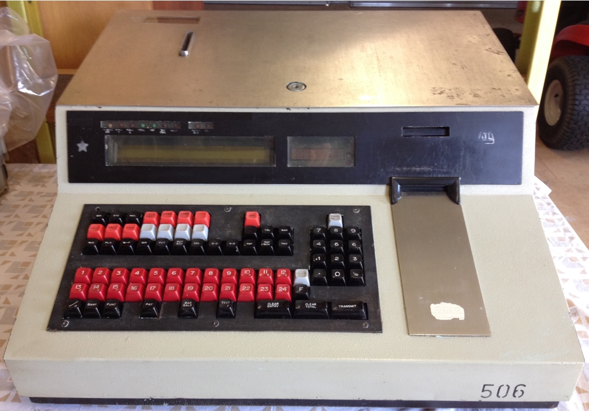
The J22 TIM (Ticket Issuing Machine)
Webmaster's Note:
The above image shows a J22 TIM which is the subject of the above documentation. The image and this paragraph do not belong to the J22 Technical Manual extract. The Processor PCB being described sits inside the near section of the TIM. Immediately underneath the keyboard is the Keyboard PCB. Beneath that and fixed to the base of the machine are two PCBs which occupy the space between the near side of the machine with the numbers 506 painted in black and the black operator display panel, which spans the width of the machine, where it rises to the large silvery grey lid. On the left hand side and spanning about a third of the width of the TIM is the Peripheral Interface PCB. To the right of this and spanning the rest of the width of the TIM is the Processor PCB being described. These boards have already been seen in the image above titled Inside the J22 with covers removed. There is a larger rendition of the J22 image in the Photo Gallery pages of this website. Click on the image at the top of the page to return to the Photo Gallery.
3.4.5 Random Access Memory Page 3/10
Four static RAMs, E66 (E43) to E69 (E46), each provide random storage for 1024 x 4-bits of memory. A chip select ( CS ) signal and a write enable ( WE ) signal are used to enable memory expansion; only the WE signal is used to read memory.
A 6-bit address, A10 to A15, plus the VMA signal is used to produce the appropriate CS signal via the one-of-ten decoders, E42 (E25) and E28 (E23), and their associated gates. (Webmaster's note: The CS signal just mentioned, stands for Chip Select. I note that in the drawing in the case of the RAMs the alternative CE has been used which stands for Chip Enable.) For example, to select E68 (E45) and E69 (E46), a logic low must be present on all bits of the address lines A10 to A15, and also VMA true. A resultant logic low will be present at Pin 1 of both E42 (E25) and E28 (E23). These are gated in E33a (E26 pins 11 and 12) to produce a logic high at Pin 10 of E34c (E31 pin 12). This is clocked via E34c (E31) by the E clock pulses at Pin 9 (E31 pin 13) to set a logic low at the CS inputs of RAMs E68 (E45) and E69 (E46).
The WE signal to the RAMs is produced by the R/ W signal. The RAM, E68 (E45), stores the four LSBs and the RAM, E69 (E46), stores the four MSBs. The 8-bit data bus, D0 to D7, is used for the transfer of data between the RAMs and the MPU. A 10-bit address, A0 to A9, is used for memory addressing.
3.4.6 Programmable Read Only Memory Page 3/11
Six PROMs E36 (E35) to E41 (E38 - only 4 in the drawing!), each provide storage for 2K x 8-bits of read only memory; the seventh PROM, E35 (E28) is used for storage of the starting address for interrupt routines (refer to sub-section 3.4.4). The memory can be erased by ultra-violet light and electrically re-programmed.
A chip select ( CS ) signal and a power down/program (PD/PGM) signal are used to read the memory. The (PD/PGM) signal is also used to set the PROMs to the power down state. In this state, the active power dissipation is reduced by 75%. The CS and PD/PGM signals are produced by the one-of-ten decoders, E42 (E25), E24 (E23) and E22 (E17), and gates E25 (E24) and E23 (E18). The resultant output of these gates (E24) is gated with the R/ W signal and the E clock pulses (E18 and E34) to produce the CS and PD/PGM signals.
A 10-bit address, A0 to A9, is used for memory addressing and the 8-bit data bus, D0 to D7, is used for the transfer of data from the PROMs to the MPU.
3.4.7 Peripheral Interface Adapter Page 3/12
The PIA, E3 (E27) provides the interface between the MPU and the Peripheral Control Board. The PIA interfaces to the MPU by the 8-bit data bus (D0 to D7), three chip select lines (CS0 to CS2), two register select lines (RS0 and RS1), a read/write line ( R/ W ), an enable line (E), and a reset line ( RST ).
The PIA is enabled by the E clock pulses and is selected by the CS0, CS1 and CS2 signals. Data transfer is performed under the control of the R/ W signal. In the READ (logic high) state the data are transferred from the PIA to the MPU, and in the WRITE (logic low) state the data are transferred from the MPU to the PIA. The RS0 and RS1 signals are used to select the various registers inside the PIA.
The PIA interfaces to the Peripheral Control Board by an 8-bit bi-directional data bus, IO0 to IO7, an Input/ Output ( I/ O ) signal, a 7-bit address, AD0 to AD6, and a Data Strobe ( DSTB ) signal. These signals are buffered by E1 (E14) and E2 (E20).
3.4.7 Bit Rate Generator Page 3/12
A 1,8432 MHz crystal-controlled oscillator is the clock source for the bit rate generator, E12 (E32). The generator provides selectable baud rate clock frequencies to drive the ACIAs, E10 (E11) and E11 (E12). The selectable frequencies and the equivalent ASCII baud rates are detailed in Table 1.
TABLE 1 SELECTED FREQUENCIES
K15(K13)
TERMINAL
PIN NO. | FREQUENCY
(Hz) | ASCII
BAUD RATE
(BPS) |
|---|
| 1 | 153.6K | 9600 |
| 2 | 76.8K | 4800 |
| 3 | 38.4K | 2400 |
| 4 | 19.2K | 1200 |
| 5 | 9600 | 600 |
| 6 | 4800 | 300 |
| 7 | 2400 | 150 |
| 8 | 758.8 | 109.9 |
| | |
Webmaster's comments:
Contemporary technologists will find the above table relating to serial line communications rather amusing, looking back at the way it was. Compare contemporary USB3 at 4.8 Gbit/s with the 9.6 Kbit/s the highest rate in the above table. I recall in the late 1970s and for all the following time I used a dumb terminal attached to a multi user system to work on software maintenance or development, that 9600 Baud was good. The other impression I had was that 1200 Baud was very slow. The only reason we would resort to 1200 Baud was to keep communications errors to a tolerable level when driving RS232 lines much further than the specifications recommended. Exceeding recommended transmission line length was only something one tolerated when forced into interfacing with equipment that was part of old installations that erroneously had been operating like this for a long time and no one wanted to spend money on an upgrade to differential lines. As for items 5 through 8 in the list, I have never had any experience with these slower rates.
There is a historic example of slower and earlier communications. I have been reading a history document by Max Burnet titled Life in the Fast ACs which provides a brief history of DEC (Digital Equipment Corporation), which was the world's number two computer company next to IBM in the latter part of the 20th Century. AC is a mnemonic for Accumulator. Max is the longest serving employee of DEC in Australia and was the CEO. The fact that DEC is the subject of this example is particularly pertinent as ATL was an OEM (Other Equipment Manufacturer or sometimes translated as Original Equipment Manufacturer) of DEC. We (ATL) based our computer totalisator systems on DEC minicomputers including the PDP8s, PDP11s, VAXs and Alphas. The PDP8 is a candidate for being the first Minicomputer class machine. The TIM in the image above, which is the subject of this page, operated in Brisbane and communicated with the host totalisator computers, which were PDP11s, designed and manufactured by DEC. The Asynchronous Communications Interface Adapter, which is described under the next heading, is the hardware in the Processor PCB, which communicated with the PDP11s. The J22 firmware used this hardware to implement ATL Digital Communications Protocol, which is based on DDCMP, to communicate with the PDP11s. Following is some historically significant information extracted from Life in the Fast ACs. Note that the baud rate mentioned is half of the lowest in the table above:
The University of Western Australia bought a PDP-6 in 1964. This was an early time-sharing machine at a time when vendors of batch-processing computers did not believe that time sharing was possible! The PDP6 was the first commercially available time-sharing machine with vendor software. When contemplating the way it was, consider that this machine's monitor (operating system) used 11K words of main memory and had 5K words of user space.
In November 1965, an historic hook-up was made by operating the PDP-6 in Perth Western Australia, from Boston Massachusetts, over a telex link. The PDP-6 was operated and programmed from Boston using a 12,000 mile communications link using a 5 hole telex code. This is believed to be the earliest example of around the world networking as Boston, where DEC's headquarters were, is about as far apart from Perth as it is possible for two cities to be distant from each other on the planet. The Telex system used a 50 baud (50 bit per second) five-bit code system!
3.4.9 Asynchronous Communications Interface Adaptor Page 3/14
The ACIAs, E10(E11) and E11(E12), provide the interface between the MPU and the host processor modem link. Each ACIA interfaces to the MPU by the 8-bit bi-directional data bus (D0 to D7), three chip select lines (CS0 to CS2), a register select line (RS), a read/write line ( R/ W ), an enable line (E) and , via the PIC (E21) (E29), an interrupt request line ( IRQ )
Both ACIAs are enabled by the E clock pulses and are selected by the CS0, CS1 and CS2 signals. The data transfer is then performed under the control of the R/ W signal. In the READ (logic high) state the data are transferred from the ACIAs to the MPU, and in the write (logic low) state the data are transferred from the MPU to the ACIAs. The RS signal is used to select the various registers inside the ACIAs. When the RS signal is logic low and the R/ W signal is logic high, the information stored in a status register is read into the MPU. This information indicates the state of the transmitter and receiver register, the modem carrier, the clear to send signal (from the modem line), and the framing error. The IRQ signal is produced by a control circuit on receipt of interrupt control signals from transmit and receive circuits and also from the modem line.
The ACIAs transmit logic formats, serialises and transmits each 8-bit (byte) of data via the TX1 and TX2 data outputs and the modem link to the host processor. The format consists of a start bit, eight data bits and a stop bit; a parity bit is not used. A request to send ( RTS ) interrupt signal is produced by the ACIAs at the start of each message. The transmit routine will not commence until the clear to send ( CTS ) signal is received from the Dual-Port Line Interface. In addition, the data carrier detect ( DCD ) signal must be valid; indicating that the modem carrier is present.
The data rates are determined by the selected frequency from the bit rate generator E12 (E32) (refer to Table 1). The ACIAs are programmed to divide the selected frequency by 16. The TX CK input is used for clocking of transmitted data and the RX CK input is used for synchronisation of incoming data. The strobing sequence is initiated eight pulses after the onset of the start pulse; this places the strobe within the 1/16th of the centre of the start pulse, and subsequently the data bits. By using the internal clock synchronisation, a 42.5% distortion is achieved. If external clock synchronisation (of divide-by-one) were used, distortion, and thus data errors, are likely to be unacceptable. (Webmaster's Note: 42.5% distortion in the good case seems high to me! It is possible this should be 4.25%! However if 42.5% produces error free communications then why worry about it! I suppose it also depends on the length of message packets, as the longer the message, the more the strobe will drift from the centre of the bit cell and ultimately encroach and drift into a neighbouring bit cell generating an error.)
The message format is programmed to suit the host processor. The maximum message length is 255 bytes, including the envelope. The MPU is programmed to expect a response within a preset period after the completion of a transmitted message. The response will be either acknowledge (ACK) or negative acknowledge (NAK). The MPU responds to a NAK by re-transmitting the previous message. If no response is received within the preset period, the MPU lights the FAULT indicator and initialises the terminal for another transaction.
A final look at the DEC Boston-Perth link
Peter Watt, who was the DEC programmer at the Perth end of this link, wrote:
"... this was the first time, as far as I know, that any computer had been used interactively from the opposite side of the globe. Certainly the first session which included the additional challenges of an international Telex link and the use of the restricted 5-bit Baudot code set."
The Telex system used a 50 baud (50 bit per second) five-bit code system which posed difficulties in generating the control codes used by all computers by then. Because 32 characters were insufficient for even just the English alphabet and digit system, the telex system used a shift convention to switch between letter shift and figure shift. The shift status affected the printer at both ends of the link, and persisted until being changed by the sending or receiving of the character which switched the system into the other shift.
The connection was half duplex; if operators typed at the same time, garbled characters appeared on each printer. During transmission, each character was represented by mark and space transitions; the line protocol was asynchronous, and the idle line sat at mark. A character was preceded by a Start bit (space), then five data bits, then 1 and 1/2 stop bits (mark). The Code used was ITA2, a derivative of the Baudot system.